
APPARATUS
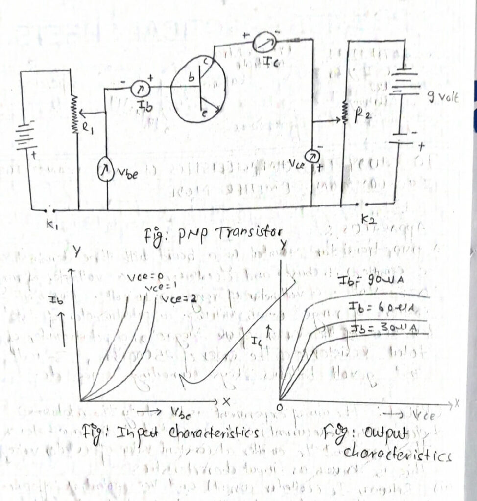
A PNP transistor Mounted on a board with three terminals Marked e (emitter), b (base) and c(collector), a voltmeter of range 0-3 volt, a voltmeter of range 0.10 volt. Two millimeters of range 0- 25 Milliamp, a potentiometer of total Resistance of the order of the order of one Megaohm, a potentiometer of total Resistance of the order of 25000 ohm, therefore volt and g volt batteries, keys connecting wires etc.
OBJECT
The aim of experiment is to study the relation :
(i) Between Ib (base current) and Vbe potential difference between the base and the emitter at constant value of collector voltage. This is known as input characteristics.
(ii) Between Ic (collector current) and Vce potential difference between the collector and emitter at constant value of base current. This is known as output characteristics.
THEORY
To study the working of PNP transistors, the emitter base circuit is forward blas with a small voltage Vbe while collector base circuit is reversed biased with a voltage Vbc. The emitter base circuit being forward biased helps the movement of holes in p-type towards the junction between emitter bases on other bands; the collector base junction being reverse biased does not allow the holes in p-type and electrons in N-type to Move towards the collector base junction. The holes in the emitter and the electron in N-type move toward the collector base junction. The holes in the emitter and the electron in the base are replaced by the positive and the negative terminal respectively of the battery Veb. On reaching the emitter base junction as fraction about 5% of the total number of holes combine with electron in the base to at neutralized
OBSERVATION
1. INPUT CHARACTERISTICS
Graph between Ie and Veb at constant collector emitter voltage least count
In Base emitter voltmeter
10 division = 0.25 volt
1 division = 0.025 volt
| S.N. | VBe | Ib vce=1.2V | Ib vce=2V | Ib vce=3V | Ib vce=4V |
| 1 | 5div x0.025=0.125V | 1μA | 1μA | 1μA | 1μA |
| 2 | 0.25V | 4μA | 1μA | 1μA | μA |
| 3 | 15X0.025=0.375 | 24μA | 2μA | 5μA | 27μA |
| 4 | 0.5V | 33μA | 15μA | 28μA | ∞ |
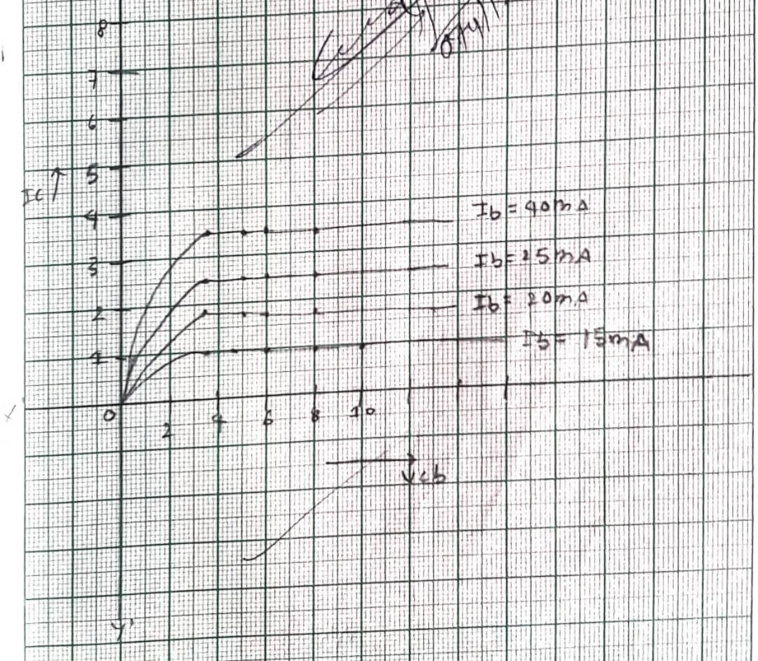
2. OUTPUT CHARACTERISTICS
Graph between Ic and Veb at constant emitter current Ic
| S.N. | Collector voltage VCC | collector current Ic (Ib=15MA) | collector current Ic (Ib=20MA) | collector current Ic (Ib=25MA) | collector current Ic (Ib=40MA) |
| 1 | 17×0.2=3.4V | 1 MA | 1.4 MA | 1.8 MA | 2.4 MA |
| 2 | 24×0.2=4.8V | 1 MA | 1.4 MA | 1.8 MA | 2.4 MA |
| 3 | 30 x 0.2=6V | 1 MA | 1.4 MA | 1.8 MA | 2.4 MA |
| 4 | 40 x 0.2=8V | 1 MA | 1.4 MA | 1.8 MA | 2.4 MA |
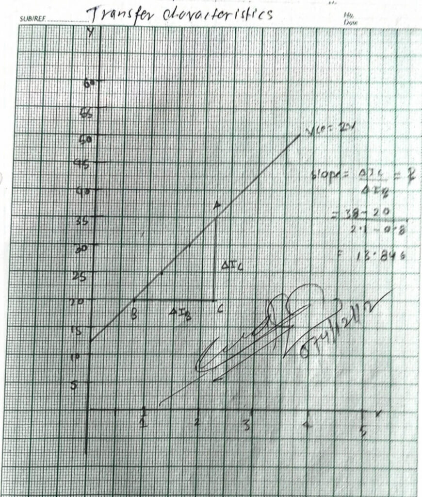
3. Transfer characteristics
Graph between Ib and Ic
| S.N. | Ib | Ic(MA) Vce= 2V | Ic(MA) Vce= 4V |
| 1 | 20 μA | 0.8 | 1 |
| 2 | 25 μA | 1.2 | 1.4 |
| 3 | 30 μA | 1.4 | 1.8 |
| 4 | 40 μA | 2 | 2.6 |
PRECAUTIONS
i) The collector voltage must not exceed the breakdown voltage for the junction.
ii) For a PNP transistor the emitter must be given a positive potential with respect to the base and the collector a negative cottage with respect to base.
iii) Correct values of blasing potential must be employed.
iv) The leads of the transfer transistor must be connected in the right way, the collector and the emitter junctions should not be interchanged.
Explore More Physics Practicals | B.Sc. 2nd Year | T.U.
- Zener Diode Characteristics & Breakdown Voltage | Experiment Guide
- Determine Specific Rotation of Sugar Solution Using a Polarimeter
- Find Impedance of LCR Series Circuit & Calculate Quality Factor
- Determine Operating Voltage of G.M. Counter | Schematic & Guide
- Verify NAND Gate as a Universal Gate Using IC Chips
- Study NPN Transistor Characteristics in Common Base Mode
- Find Wavelength of Light Using a Diffraction Grating
- Find Wavelength of Sodium Light Using Newton’s Rings
- Determine Viscosity Coefficient of Water | Poiseuille’s Method
- To Determine Surface Tension Using Capillary Tube Method
- Determine Young’s Modulus by Bending Beam Method | PDF
- Determine Moment of Inertia & Angular Acceleration | Flywheel
- Determine Acceleration Due to Gravity & Radius of Gyration | Bar Pendulum
- Determine Modulus of Rigidity Using Maxwell’s Needle | PDF
- Study Charging & Discharging of Capacitor | Find Capacitance